Breadboard computer pictures
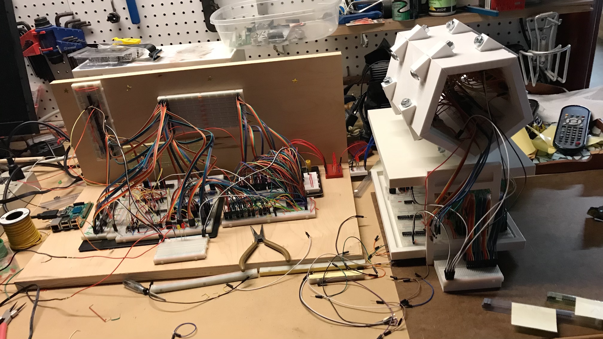
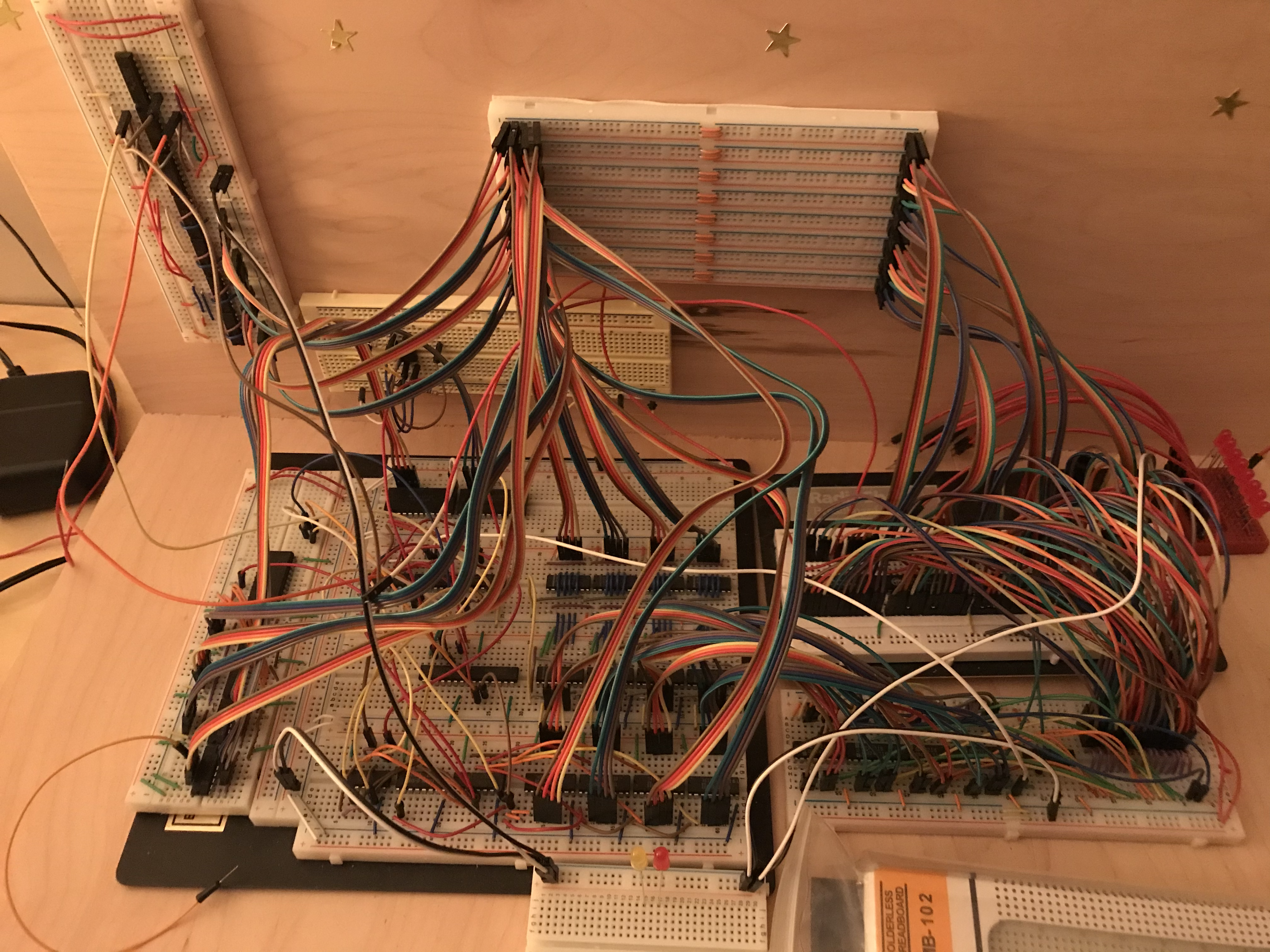
An image of the whole thing, albeit not connected together.
The clock- a 555 IC in astable configuration
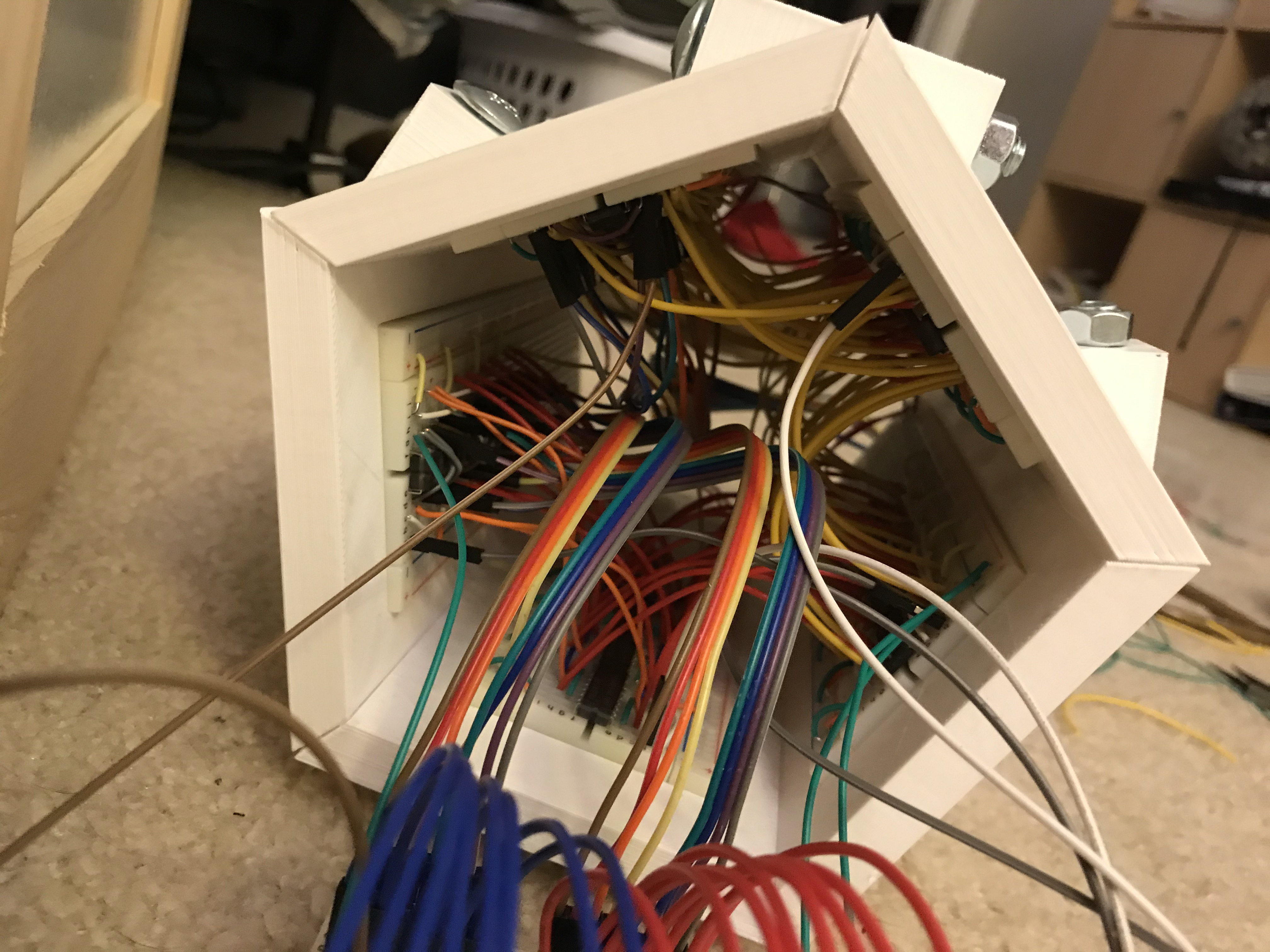
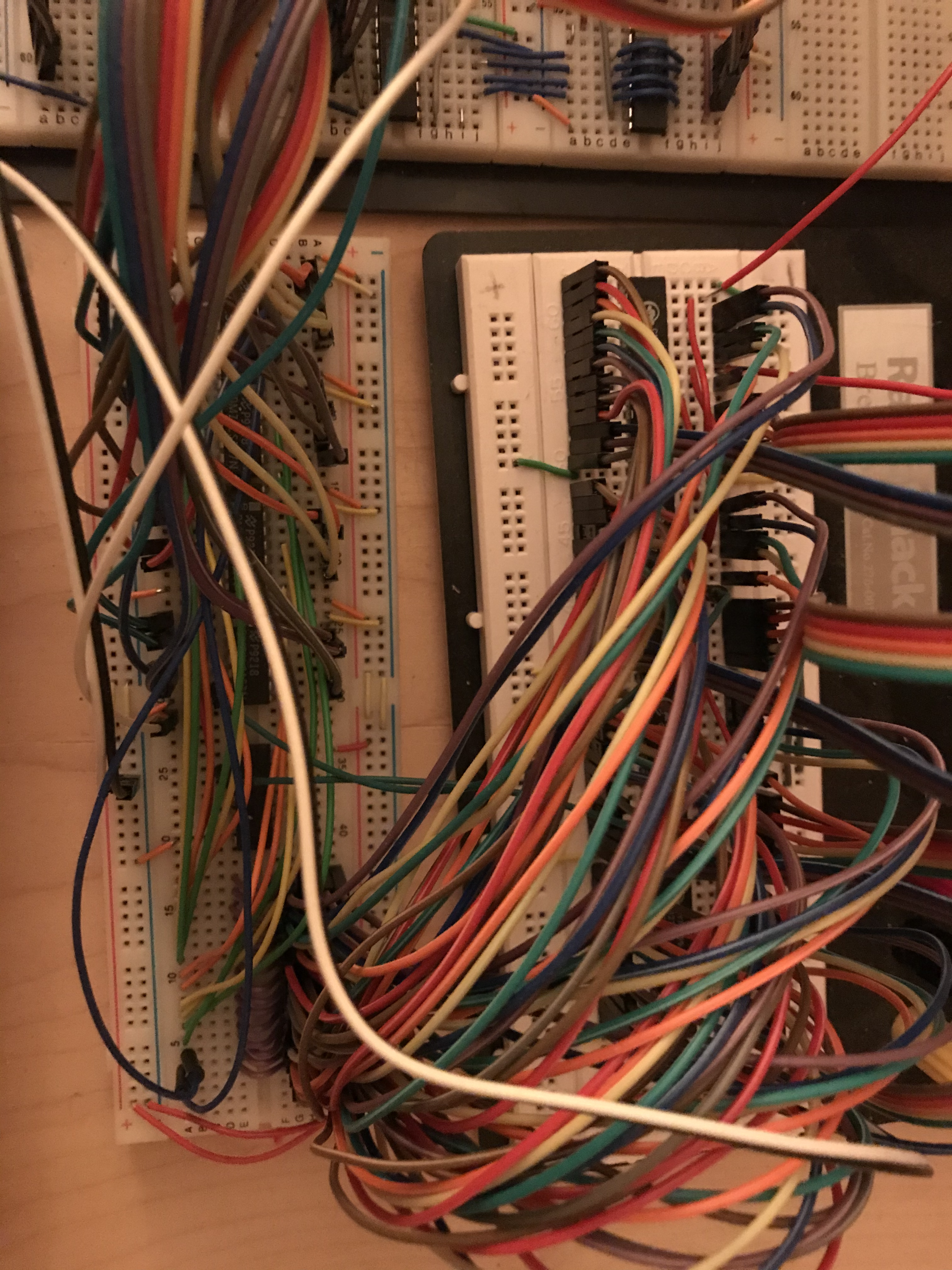
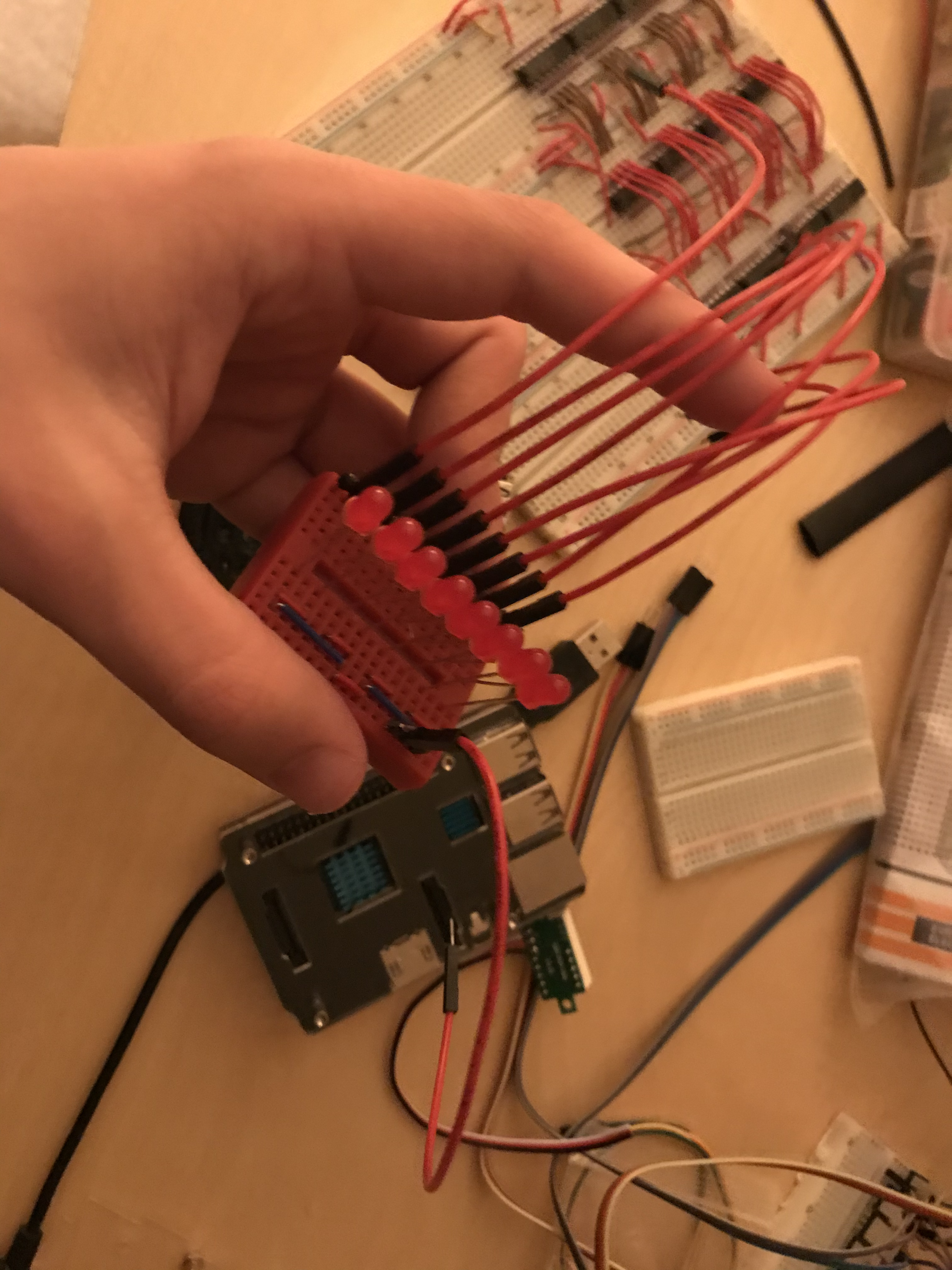
This component is a series of multiplexers that handle bitwise shifting. I thought it would be cool to make it circular, since it eliminates any wires having to travel back to the other side of the board, but I ended up feeling very silly wiring the thing up when all the breadboards were inaccessible.
Two registers- the address register that controls what word of memory is being accessed by RAM, and another, general purpose register that can be used for rearranging data in other registers.
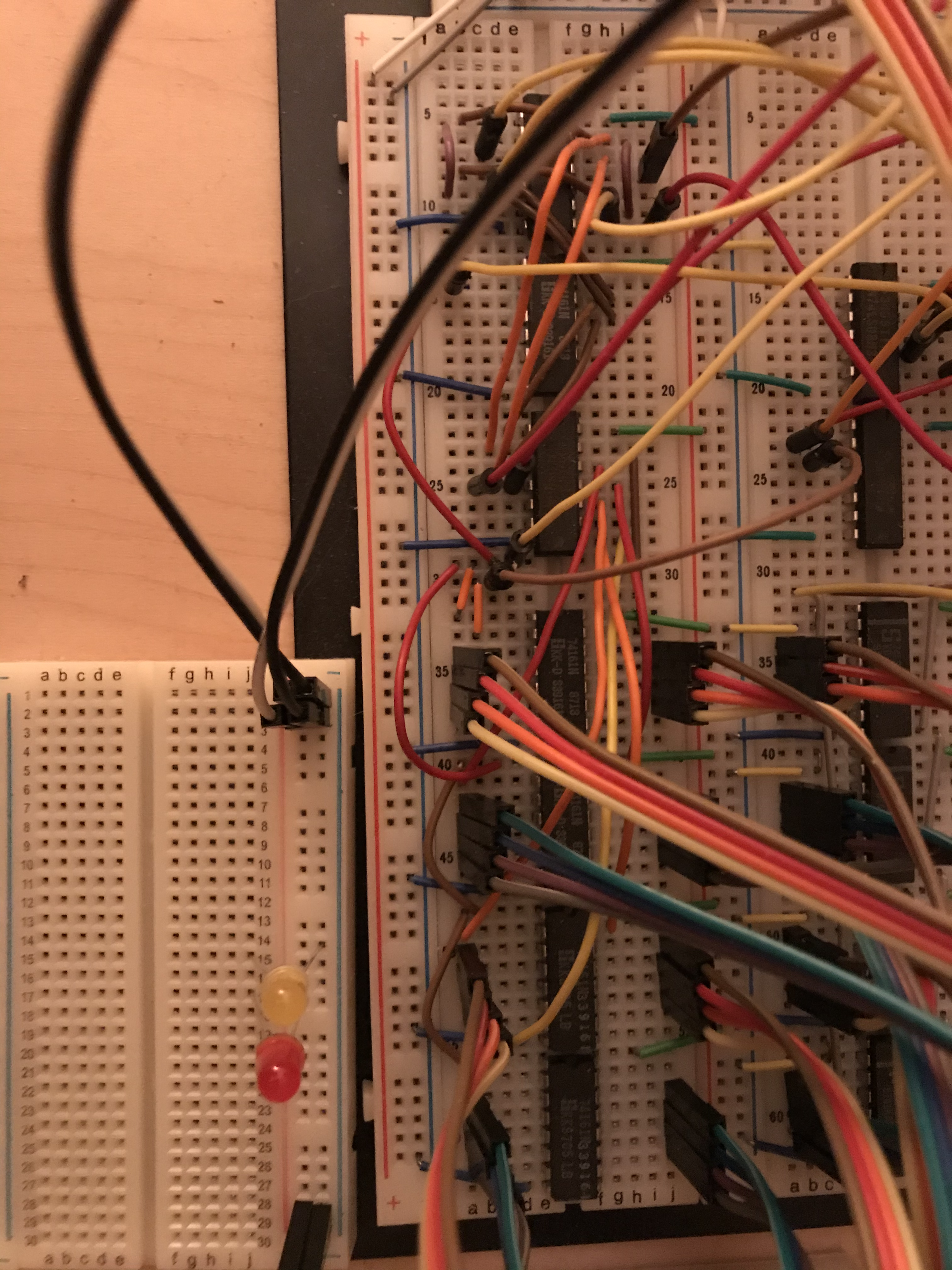
Here you can see the RAM, and also the multiplexers that head into the RAM that decide between listening to the address register, for accessing program memory, and listening to the instruction counter, for accessing the next instruction that should be executed.
MOSFETS to allow the raspberry PI to initialize the machine state.
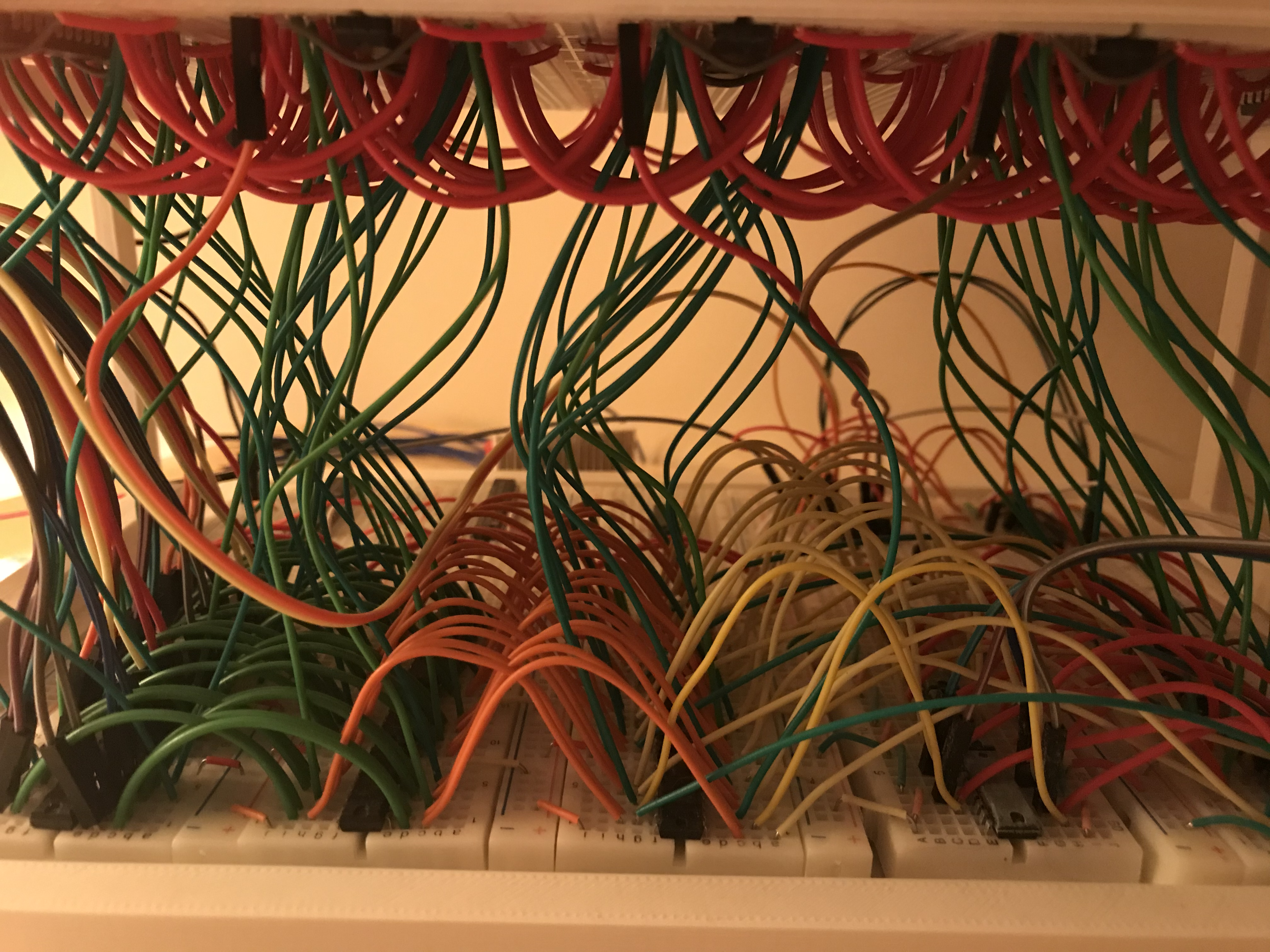
Again, I 3D printed a setup that I thought would be cool, and then it bit me during wiring when I realized that none of the breadboards were accessible. This is the full adder/subtraction circuit. It also allows the computer to perform bitwise binary operators (except for bitwise shifting.)
A cleaner view of the registers that feed into the ALU. All binary operations are performed on the values stored in these registers.
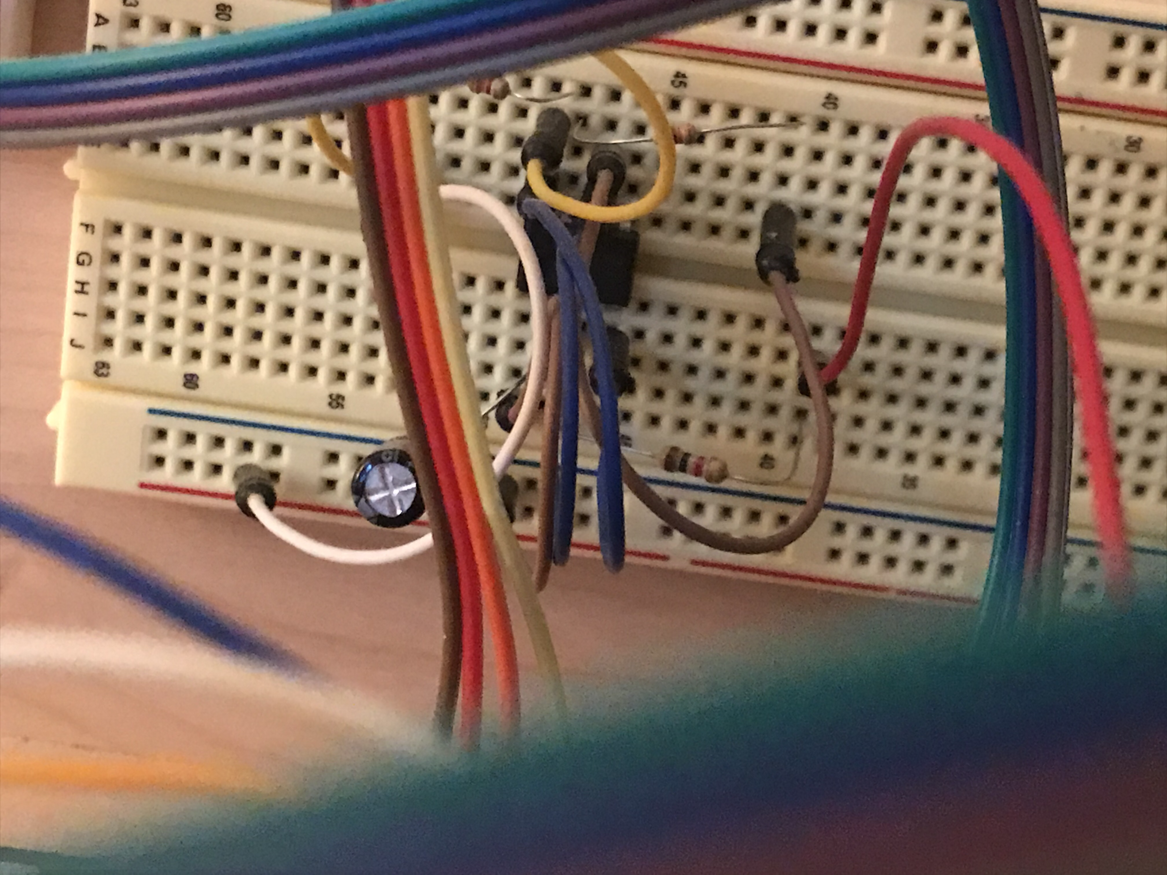
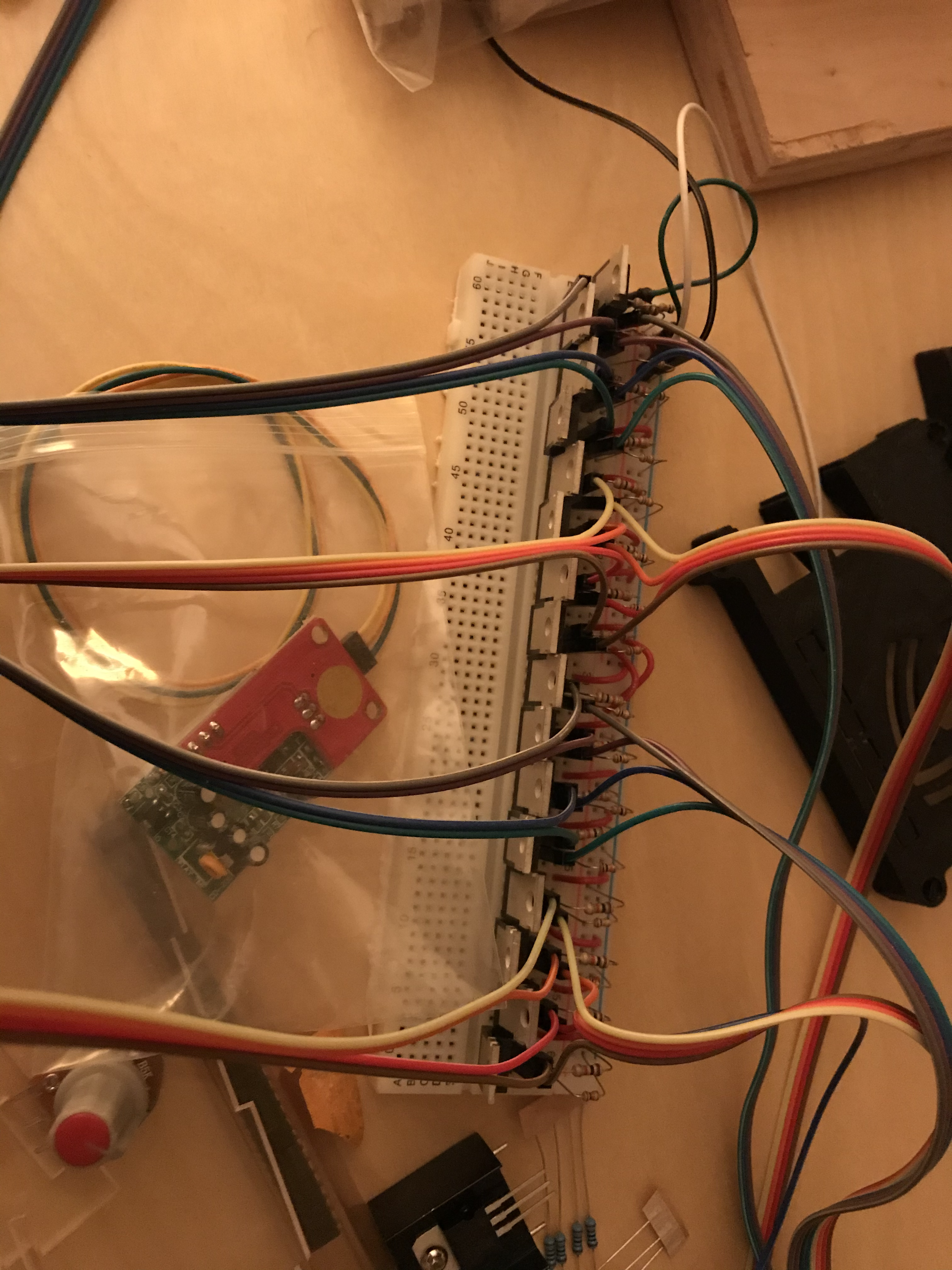
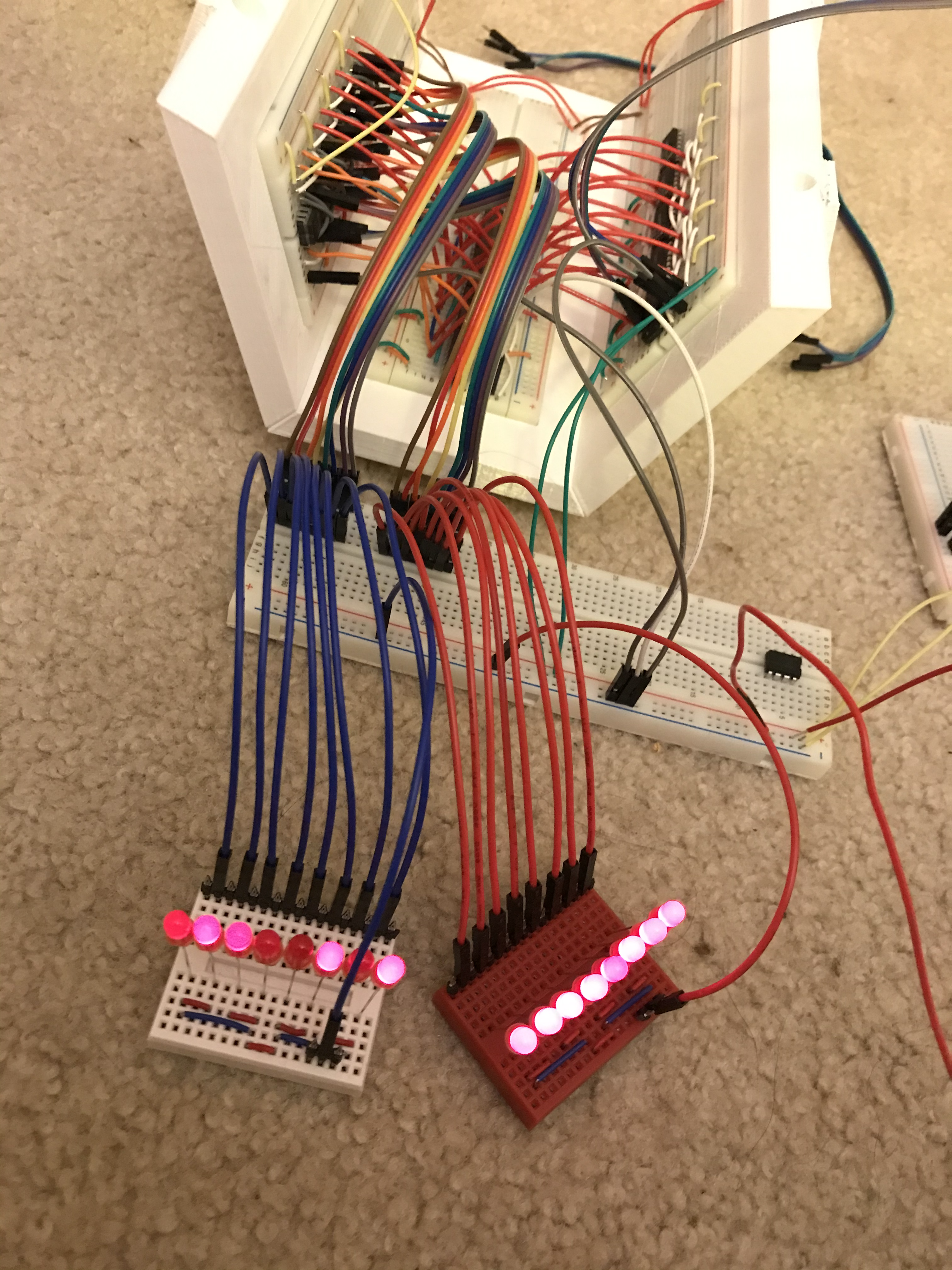
This is the doodad I would use to test parts of the circuit. They would act as a pulldown resistor, which would sometimes disrupt the circuit if I was measuring an intermediate step in the circuit, so I had to test everything modularly.
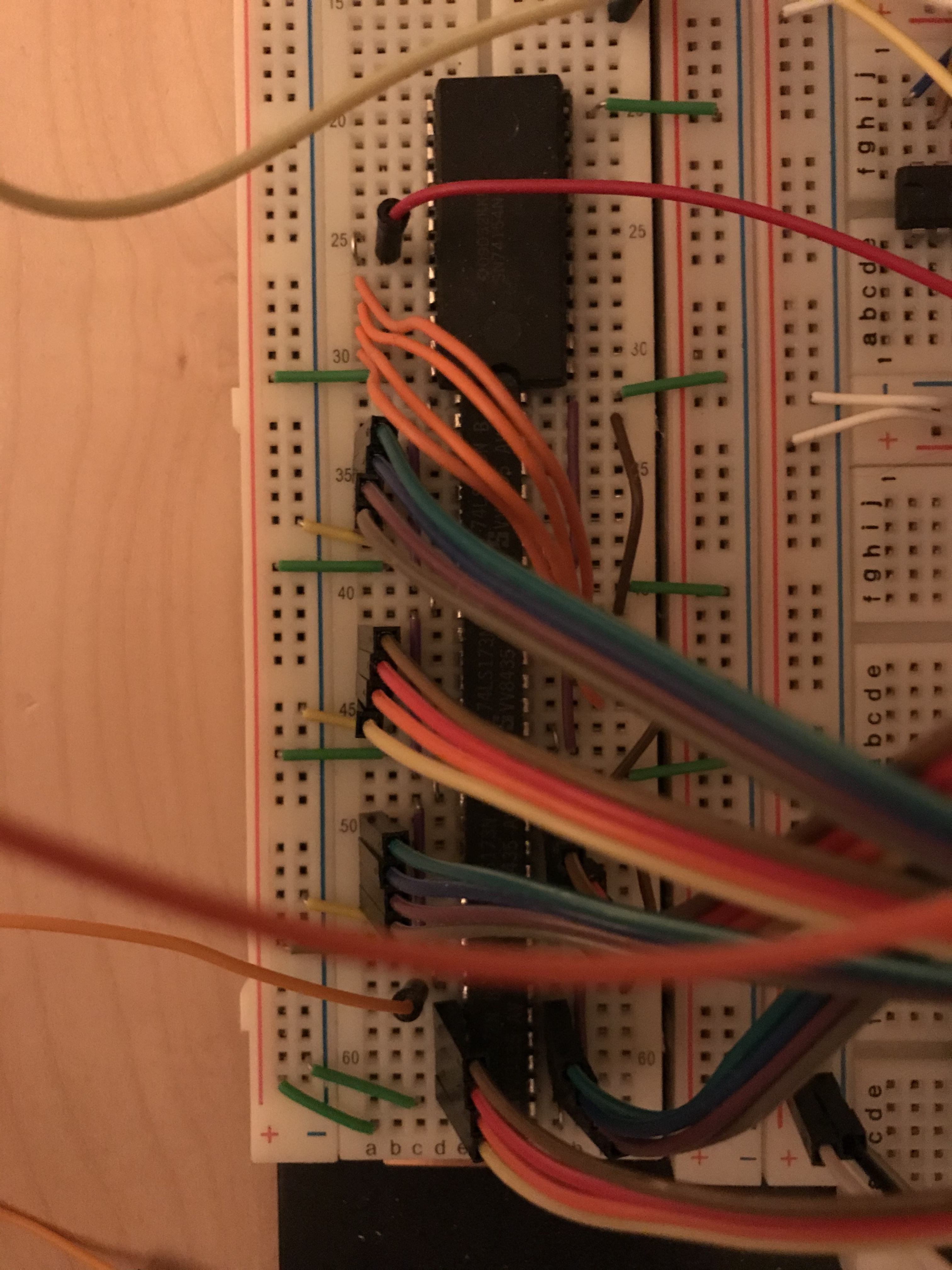
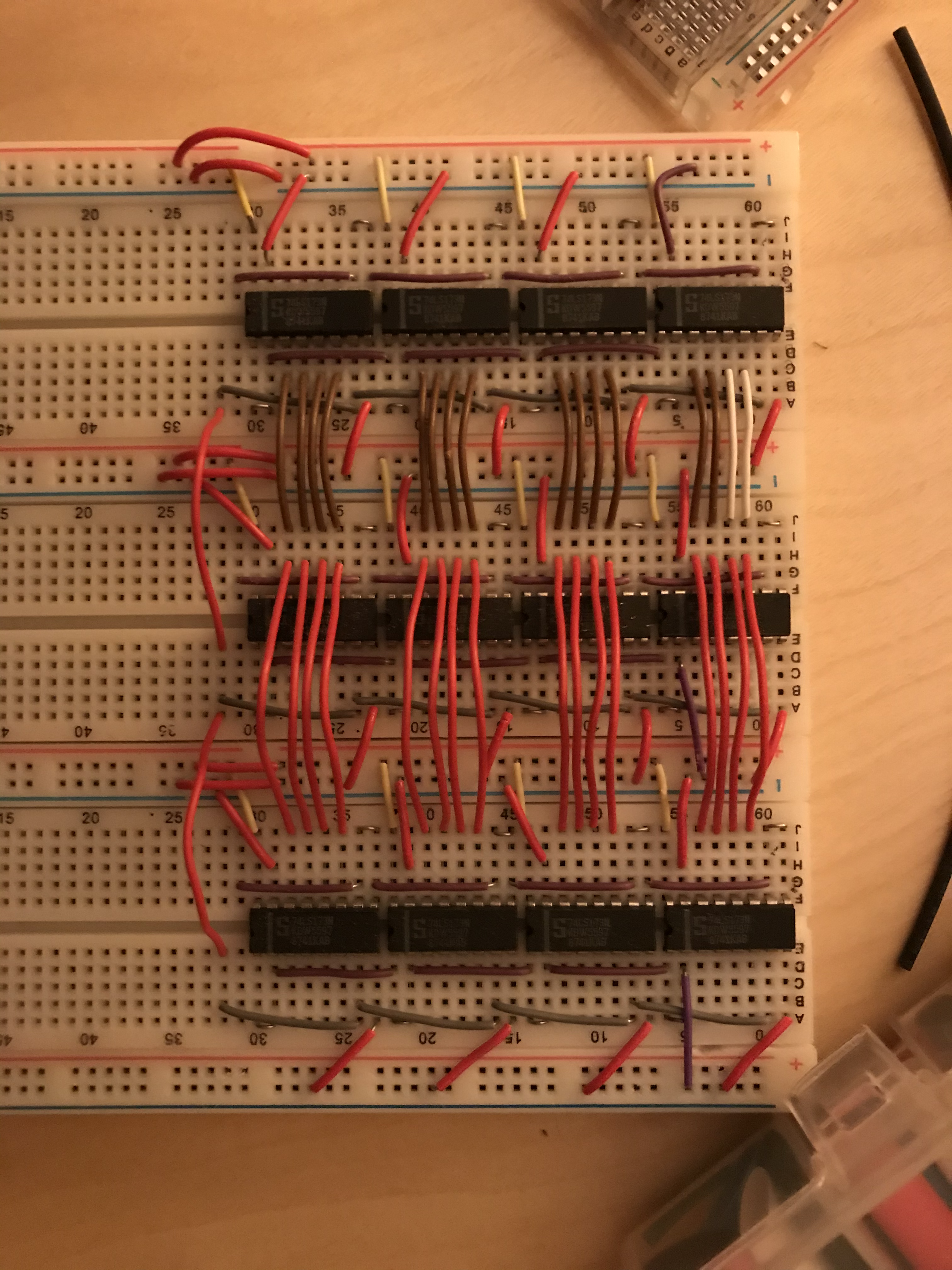
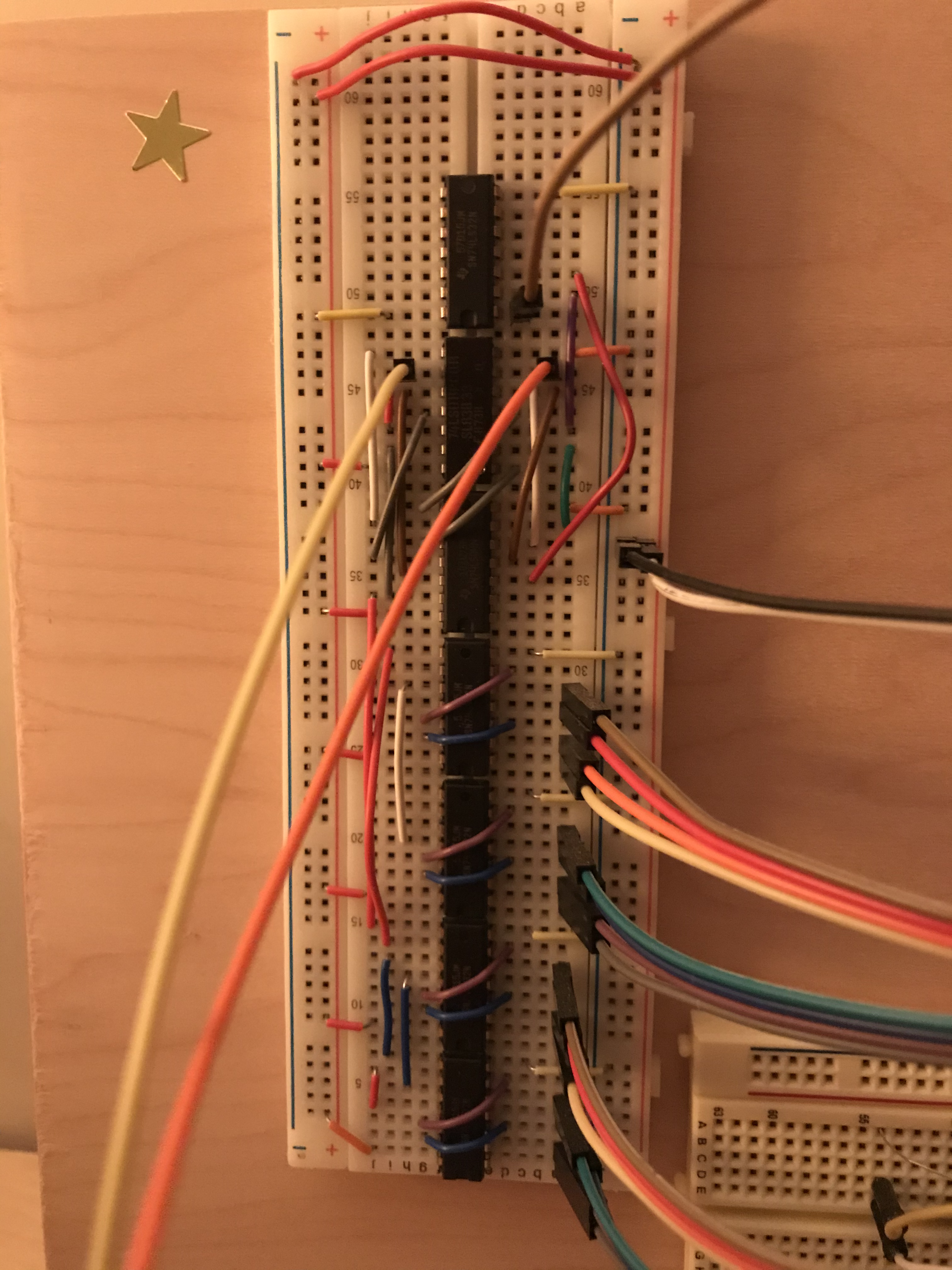
This is the instruction buffer and the decoder that I used to decode certain instructions.
This is the instruction buffer and the decoder that I used to decode certain instructions.
Overall view of the RAM and instruction handling portion
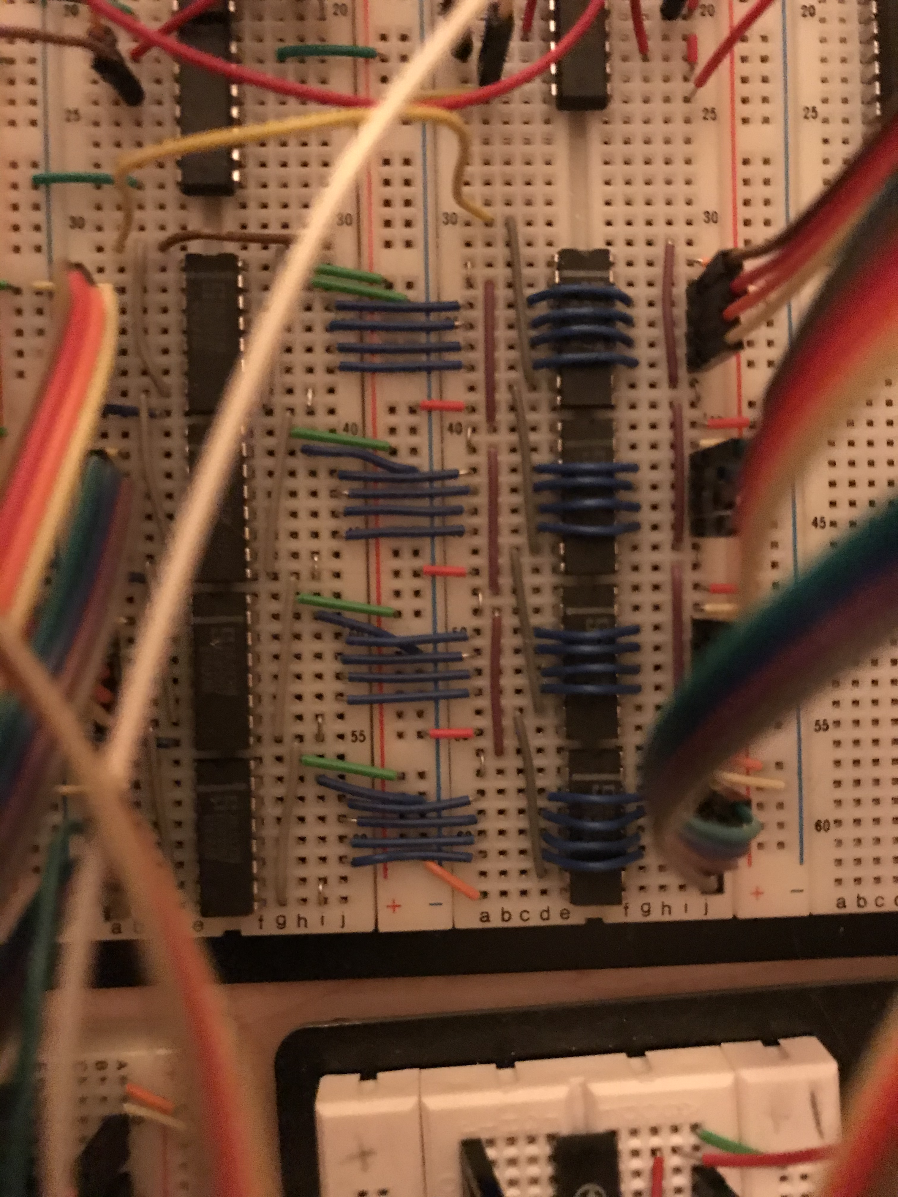
Decoders used to select input and output registers during the appropriate instructions
The program counter (and inverters because the carry signal was active low)
Correct operation of a small portion of the bitwise shifting circuit
A series of OR gates and a latch. This stores whether or not the last operation was nonzero, for the purposes of conditional branching. The conditional skip operation uses this to determine whether or not to skip.