Breadboard computer ALU
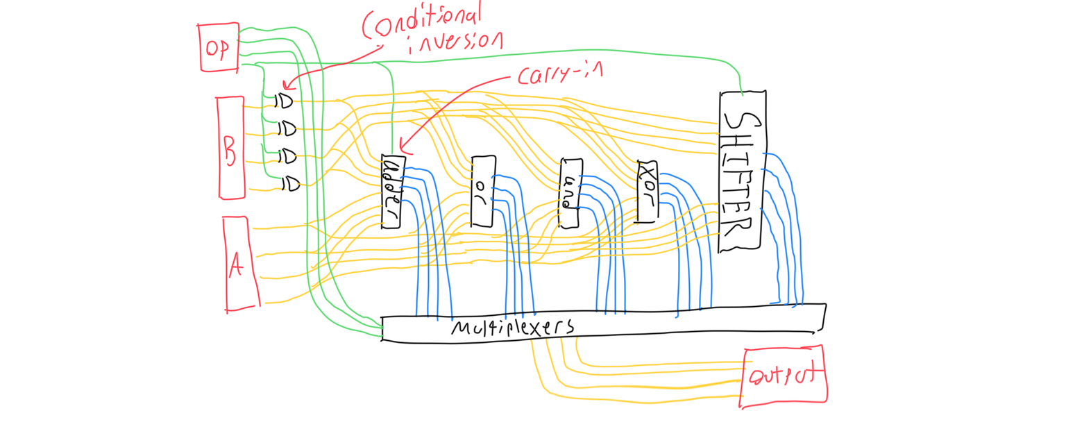
The alu is the largest part of the computer. Its purpose is to perform binary operations on buffers A and B. To support all of these different operations across a reasonable amount of board space, an effective strategy can be used. The eight operations are arranged in such a way that the rightmost operation selection bit always involves inverting buffer B before performing one of the four binary operations. The rightmost bit is also the full adder’s carry in, which implements subtraction via two’s compliment. The other two operation selection bits select which operation to perform after conditional inversion of B.
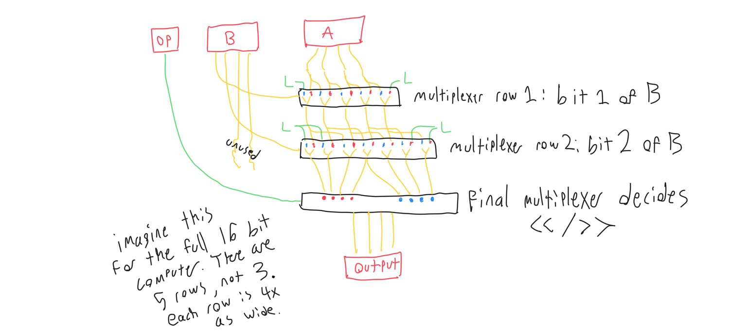
While bitwise or, and, xor, and even full adders come in IC chip form, bitwise shifting must be assembled out of smaller elements. Specifically, many multiplexers. The module shown above labeled ‘shifter’ follows the schematic below. Even the simplified schematic bears explaining- each row of multiplexers may translate the word to the right some amount. The first row translates the bus 1 signal over, the second one translates it 2 over, the third translates it 4 over, and so on. There is one more multiplexer at the end that decides whether to listen to the right side or the left side of the message. If the op input is false, the last multiplexer would listen to the red inputs, which results in left shift behavior. When it is true, however, the last multiplexer would listen to the final inputs in the message. This is coupled with an understood inversion to B that occurs outside of the shifter, so for example a right shift by zero would shift the message as far as possible because the bitwise inversion of zero is each bit held true, and then the final multiplexer would collect the message at the far end, leaving it unchanged. Right shift behavior is correctly achieved when the op input is true.