Breadboard computer operations
I planned to support a limited but easily Turing-complete opset, settling on the following list of operations for the breadboard computer:
- SET: sets a given buffer (not ram) to the word after the current instruction, and then skips over it to avoid interpreting the word as an instruction.
- MOV: moves a word from one buffer to another, or from a buffer to ram at the address pointed to by the address buffer, or from ram at the address pointed to by the address buffer to a buffer.
- ALU: performs an indicated operation on buffers A and B and stores the output in a designated location.
- SKP: selects an indicated buffer (or ram) and skips the next operation only if that buffer is non-zero.
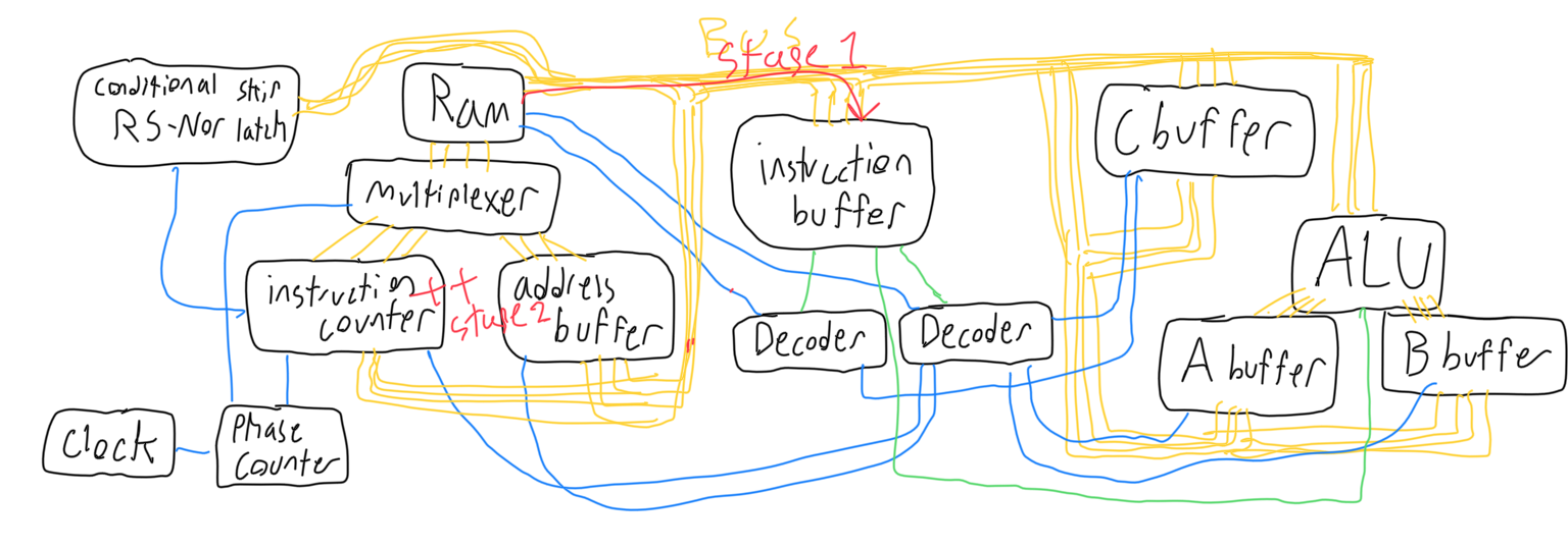
To select a buffer to input to or output from, two decoders are used. Decoders accept some binary input and ‘select’ one output to be held high while the other outputs are held low. One decoder is used to select an input and another decoder is used for outputs. Instructions are interpreted the following way:

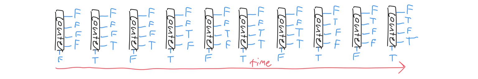
It is important to note the lack of a JMP instruction. This is because the computer achieves this by having the instruction counter as a possible input. This way, the computer can use a SET instruction to jump to a predefined location in the instructions, or a MOV instruction to get a location from RAM or the C buffer and jump to a computed location. The phase counter is a counter that I use to segment each instruction into four stages. The counter counts to four in binary, increasing by one each time it gets an input, and resetting once it reaches four. Each different number on the counter puts the machine in a different stage. The first and second stages are simple because they are the same for each different instruction, but the third and fourth depend on the instruction that the machine is currently on.
On the first stage, the machine sets the multiplexer to listen to the instruction counter, sets the RAM to output, and sets the instruction buffer to read. This effectively reads the current address into the instruction buffer. On the second stage, the machine increases the instruction buffer.
The instruction buffer then differentiates the next two stages.
-
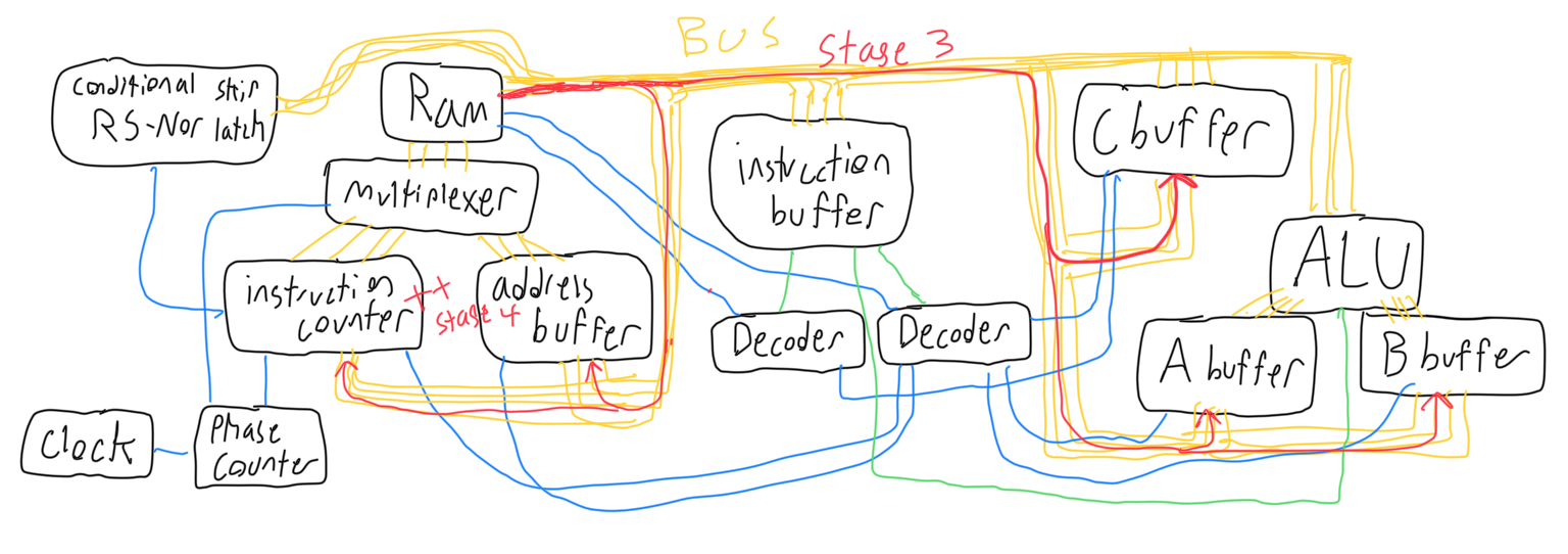
For the SET operation, the third phase keeps the multiplexer listening to the instruction counter and sets the ram to output. The input decoder is used to determine the buffer that will be set to input. The fourth phase increments the instruction counter once more.
-
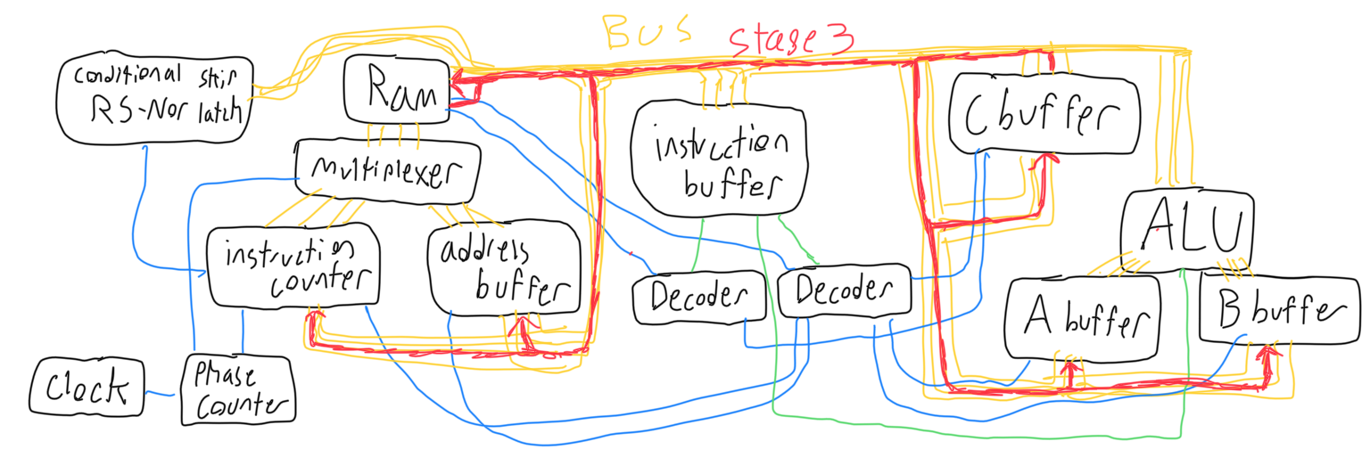
For the MOV operation during the third phase, the output decoder is used to determine which buffer (or ram) will be set to output, and the input decoder is used to determine which buffer (or ram) will be set to input. The multiplexer will be listening to the address buffer during this phase. The fourth phase is empty.
-
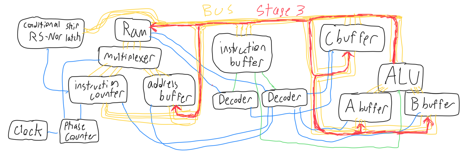
The ALU operation uses the output decoder to determine which operation to tell the ALU to perform, and the input decoder to determine which buffer (or ram) to set to input. The fourth phase is empty.
-
During its third phase, the SKP operation uses the output decoder to determine which buffer (or ram) to set to output, and the rs-nor latch is set to input. During fourth phase, the instruction counter is incremented if the nor latch is high.
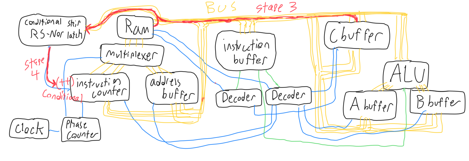
The conditional skip latch was used to remember the state of the bus during SKP phase 3 so that during phase 4 it may or may not be incremented. I could have used one bit of a buffer IC, but at the time I didn’t have extra buffer ICs, only hex inverters.

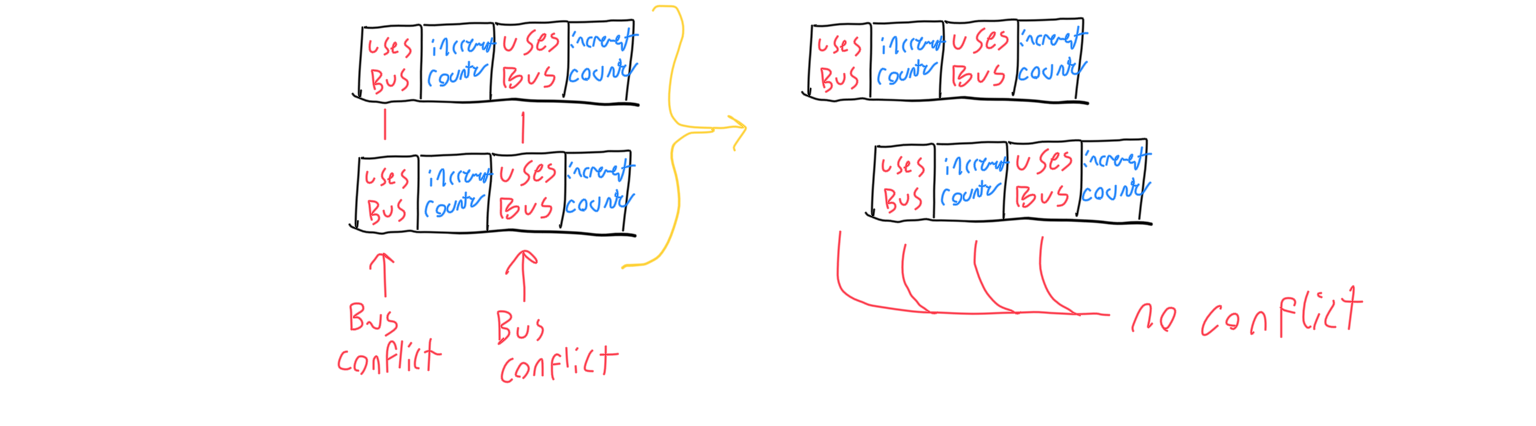
It is important to note that no matter the instruction, the bus is only used during the first and third phases, while the second and fourth are used for incrementing the instruction buffer only. Though I never got around to it, this was so that the machine could have two cores. Since both cores only touch the bus on their first and third phases, they could coexist if one’s even phase lined up with the other’s odd phase. Each core would have its own instruction counter, instruction buffer, input/output decoders, address buffer, conditional skip latch, and its own A,B, and C buffers. A hefty number of multiplexers would need to be in place to switch between each set of buffers to select which core was interacting with the bus. Even just one core quickly became a large undertaking, though, so I let the two core design stay an idea.